
Lightspring raises €3.5M to tackle photonic chip manufacturing bottleneck
Tech.eu Cate Lawrence
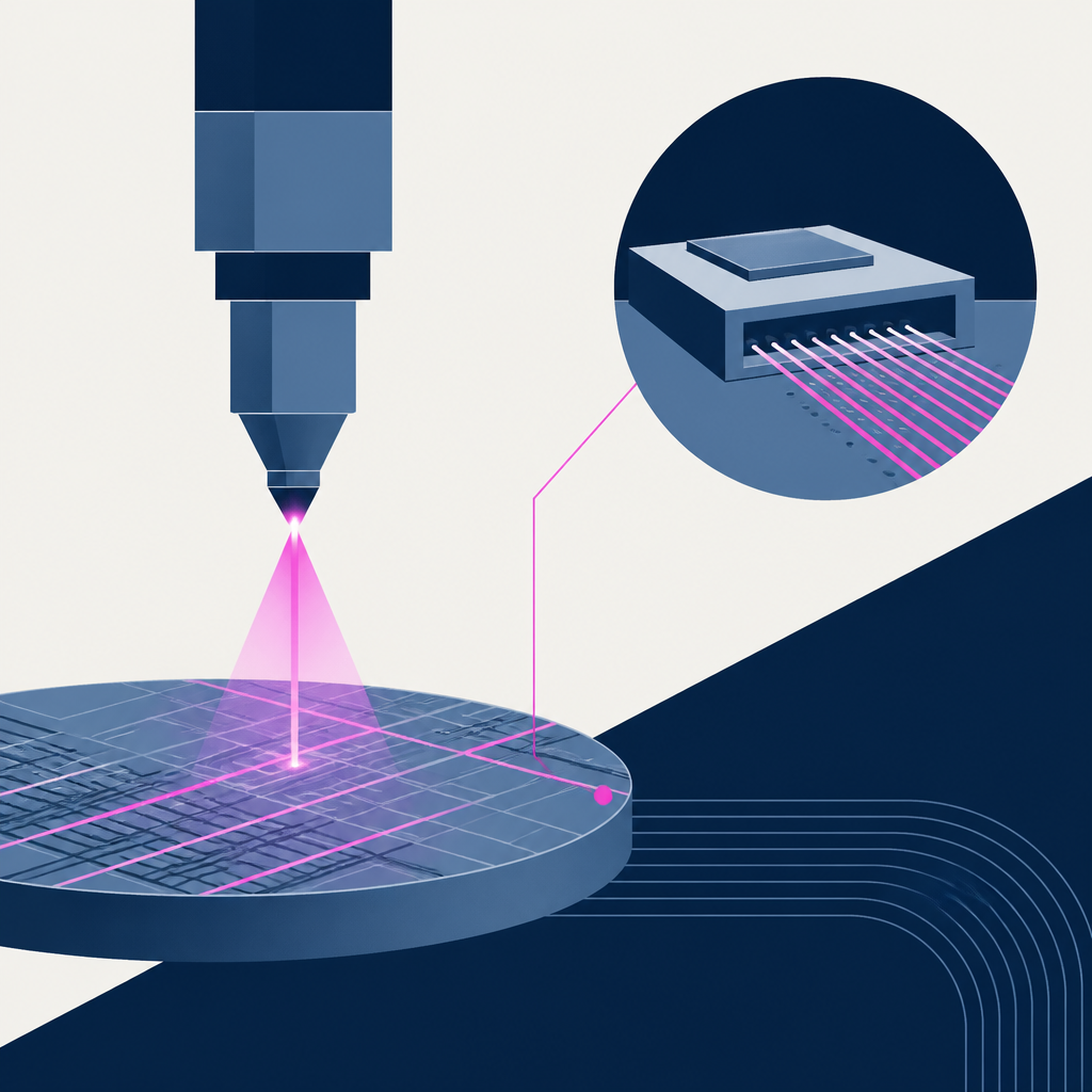
Lightspring raised over €3.5M to industrialise photonic chip packaging. It wants to make the hardest, costliest step in the chain reproducible.
Based on reporting by Tech.eu, Cate Lawrence — read the original for the full story.
Summary, retelling and take written by AI under human oversight; images are AI-generated illustrations. How we work · Report an error
French startup Lightspring has closed a €3.1 million seed round led by Atlantic and OVNI Capital, with backing from Concept Ventures, Ixcore, Plug and Play Ventures, and industry angels. It also picked up a grant of €350,000 and additional public innovation funding, bringing total financing to more than €3.5 million.
The company is going after a stubborn bottleneck in photonic chips: optical packaging. PIC fabrication is already handled by a small set of mature foundries, but assembly and optical packaging still take around half of a chip’s cost, compared with roughly 20 per cent for the foundry work. The problem is especially messy at the fibre-to-chip stage, where parts are aligned one by one with micrometre precision, adding typical losses of 2–3 dB and dragging down throughput and yield.
Lightspring’s answer is to build the optical interface directly on the chip using 3D lithography, specifically two-photon polymerisation. That lets it print microlenses, 3D waveguides, and beam-shaping structures in a single step. The company says the process can handle fibre-to-chip, laser-to-chip, and chiplet-to-chiplet coupling, with target losses below 0.5 dB per interface. It also aims to remove active alignment entirely and keep the approach both materials-agnostic and equipment-agnostic.
The pitch is as much about industrial workflow as physics. Lightspring says its core IP sits in the design layer, through a first Process Design Kit dedicated to 3D optical coupling, along with software tools and qualified fabrication recipes. The technology comes out of research at FEMTO-ST Institute in Besançon, where co-founder Daniel Brunner is CNRS Research Director. Grégoire Bonnat, the company’s co-founder and CEO, says the money will help turn a lab result into a qualified industrial building block.
The funding will go toward the PDK, design tools, team growth to 12 people, co-design work with industrial partners, and qualification of the fabrication process for industrial use. Atlantic’s Quentin Calleja and OVNI Capital’s Thomas Renaudin both frame the bet the same way: AI hardware keeps pushing optics closer to compute, but nobody has had a good way to manufacture that optical interface at volume. Lightspring is trying to become that missing layer.
My take — AI-written commentary, not fact-checked reporting
This is the kind of deeptech bet Europe should be making: boring on the slide deck, crucial in the factory. Everyone loves to talk about AI chips, but packaging is where the bill shows up. If Lightspring can really make optical coupling reproducible, that beats another round of glossy inference hype any day.
Read more about this at: Tech.eu
Related stories
 Solinide raises €4M to commercialise photonic chip tech for data centres
Startups Magazine ·
34
iPronics: Spanish Photonics Startup Raises $125 Million From Nvidia and Others
Trending Topics · 2 weeks ago ·
31
Solinide raises €4M to commercialise photonic chip tech for data centres
Startups Magazine ·
34
iPronics: Spanish Photonics Startup Raises $125 Million From Nvidia and Others
Trending Topics · 2 weeks ago ·
31
 Solinide closes €4M to commercialise photonic chips for AI data centres
Tech.eu · 1 month ago ·
31
Solinide closes €4M to commercialise photonic chips for AI data centres
Tech.eu · 1 month ago ·
31